Sub-Nanometre Dielectric Bowtie Cavities from Single Silicon Atoms: A New Approach to the Manufacturing of Novel Nanostructures
Recent developments have brought miniaturization to the centre stage also in photonics because it is required for realizing dielectric bowtie cavities5 with ultrasmall mode volumes—a regime previously believed to be accessible only in plasmonics19,20. The existence of dielectric cavities with mode volumes below the diffraction limit was predicted21 in 2005 but demonstrated only very recently5, in part because realistic designs were missing and in part because experimental progress was impeded by the extreme requirements on the nanofabrication. Light andmatter interact with each other through field discontinuities at material boundaries, and the promise of a new class of light–matter interactions is demonstrated by the formation of Dielectric bowtie cavities. The width of the bowtie is the most crucial parameter because it determines the field enhancement22. Although minor improvements along this route may be possible, it appears pointless to try to scale conventional etching to atomic dimensions with aspect ratios exceeding 100 because of the confinement of light demonstrated in the first experiment. Features that have low refractive index are a challenge to fabricate, but they are needed for some of the most radical applications of nanostructures, such as bulk non linearities operating at the single-photon level25. While top-down nanofabrication in modern foundry production allows defining the position of edges with both precision and accuracy (disorder) at the level of a single silicon atom29, the resolution limit (the smallest possible linewidth) of approximately 50 atoms has so far hindered such developments, see Supplementary Information Section 1.
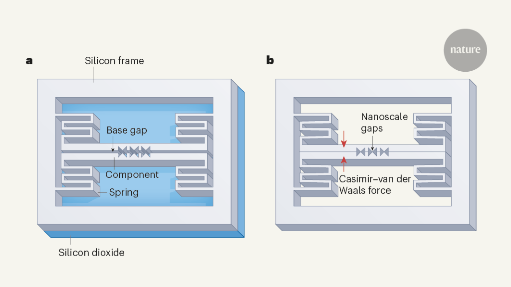
Here we propose and demonstrate a new approach to the manufacturing of semiconductor devices. It’s possible to build devices with unprecedented dimensions using the surface forces which act on objects more than 10 times the size of a single atom. Our experiments enable controlled, deterministic and directional collapses to be used to fabricate miniatureaturised devices with a few- or even sub-nanometre dimensions.
The fabrication of functional materials and devices at the micro- and nanoscale is usually done using a top-down approach and using various effects, such as van der Waals or hydrogen-bonding forces. The bottom-up approach has enabled research on a wide range of devices with near-atomic dimensions. For research and technology that rely on strong field gradients or quantum effects, miniaturization is crucial. The industry plan predicts that there will not be a minimum half-Pitch or physical gate length below 8 nm until 2037. Synthetic self-assembly is far from being able to replicate the Centralized and Scalable self-Assembly in biological systems. A practical consequence is that a wealth of research on bottom-up nanotechnology for information technology always had to rely on top-down technology for the interconnect architecture. For example, lithographically defined wires or waveguides are needed to contact single-molecule devices14 or single-quantum-dot devices7. Combining the scalability of top-down planar technology with the resolution of bottom-up approaches would open vast perspectives15, but they are commonly considered disjoint. Self-assembly has been explored for fabricating origami-like structures in microelectromechanical systems16, which enable unique geometries but not nanoscale dimensions. Combining nanoscale self-assembly with planar technology has been found to be difficult, but a pathway for their direct integration has yet to be found.